Carnegie Mellon University
—
—
—
Search
Search
Search this site only
Claire & John Bertucci Nanotechnology Laboratory
College of Engineering
College of Engineering
›
Claire & John Bertucci Nanotechnology Laboratory
›
Facilities & Equipment
› Elionix ELS-G100 Electron Beam Lithography System
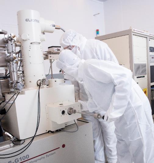
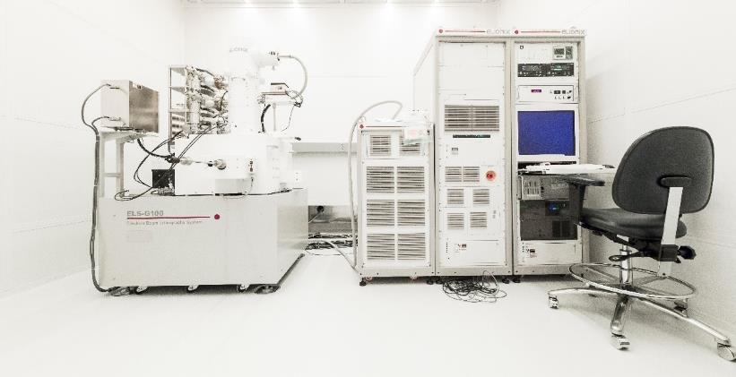
Elionix ELS-G100 Electron Beam Lithography System
Overview
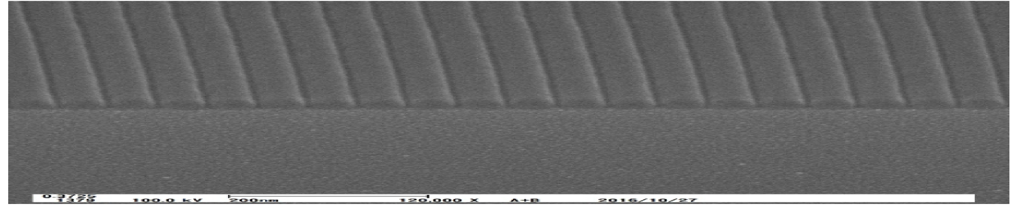
100kV and capable of patterning features down to 5 nm with high alignment accuracy (20nm or better) and over large wafer area
Beam currents up to 100nA for high throughput on wafers up to 6”
Please consult
Nanofab staff
for process specifics.